
JOHN TIMMER
Source: arstechnica.com, May 2019
It can do AND or OR logic in a single transistor, switch states using light.
With the development of carbon nanotubes and graphene, scientists were given an entirely new collection of materials to work with: sheets and tubes that could be consistently made with thicknesses roughly those of individual atoms. These materials hold the promise of building electronic devices with dimensions smaller than is currently possible through any other process and with properties that can be tuned by using different starting materials.
So far, most of the attention has gone to re-creating new versions of familiar devices. But a new paper by a group of researchers in Shanghai looks into what can be done if you’re not constrained by the sorts of devices we currently make in silicon. The result is a device that can perform basic logic in half the transistors silicon needs, can be switched between different logical operations using light, and can store the output of the operation in the device itself.
OR or AND?
Computer instructions can be distilled down to a series of simple logical operations. Of these, the simplest are AND and OR. AND produces a value of 1 only if both of its two inputs are also 1; OR does so if either of the two inputs are 1.
But there’s a mismatch between these logical operations and what we can do with silicon: a silicon transistor can only take input from a single source instead of the two required here. As a result, these operations require two transistors on a processor.
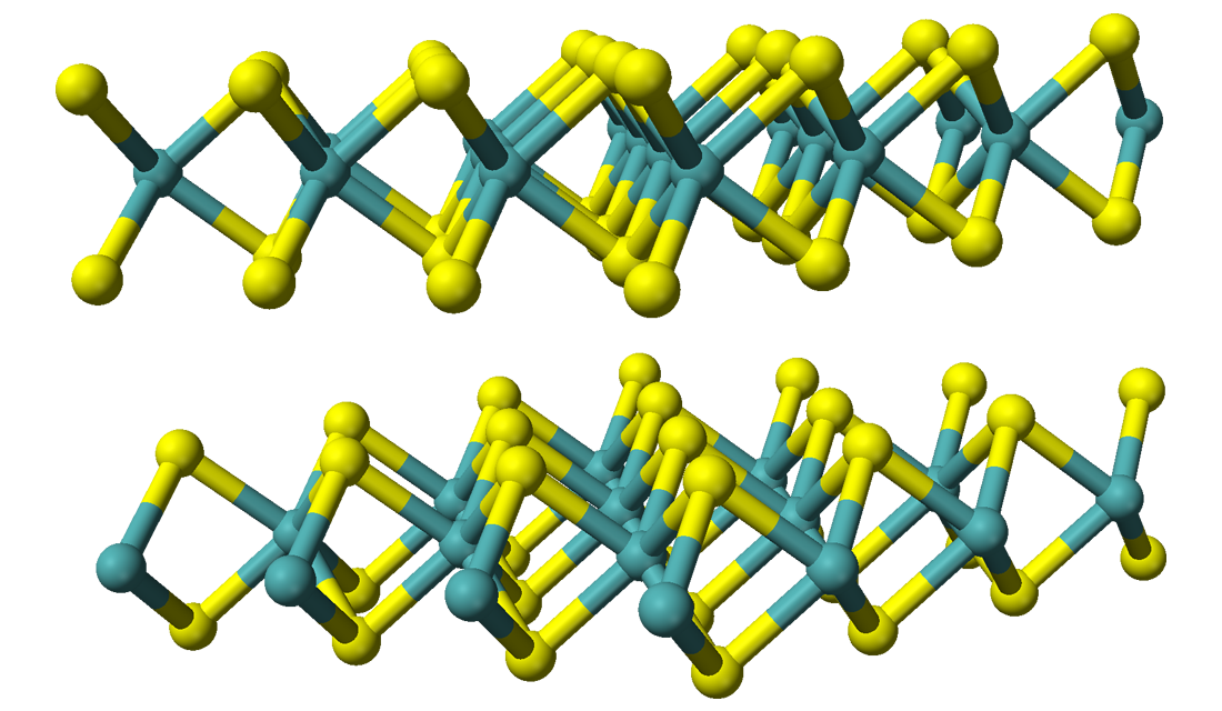
Transistors made of an atomically thin material can have fundamentally different structures, though. To test some of these, the researchers used molybdenum disulfide (MoS2), which forms graphene-like sheets slightly thicker than its component atoms. Like silicon, MoS2 is a semiconductor; unlike silicon, putting input gates both above and below a single layer of the material is relatively easy to do. This allows for the layer to take input from two different sources, making it a direct match for the logical operation’s input.
Better yet, the researchers found they could make extremely similar devices that performed different logical operations. MoS2‘s individual sheets may be atomically thin, but it’s possible to stack multiple sheets on top of each other. Initially, with just a few sheets stacked, the MoS2formed a single semiconducting layer that would switch to conducting only if the gates both above and below it were in the “on” state. This makes for a perfect match to the AND function.
But keep adding layers, and the thickness would eventually reach a point where the upper and lower gates could independently control the conduction of the sheets of MoS2 nearest them. The authors compared it to having two “channels” on the same device. If either of those channels was set to “on,” then some current would flow through the device, making its global state “on.” This was a perfect match to the logical OR function.
The critical thickness turned out to be four nanometers, or less than half the size of existing features in cutting-edge chips. If the MoS2 sheets were stacked into a layer above 4nm, then the transistor would behave as an OR gate. Below that thickness, and it would perform AND operations.
Light and memory
At this point, the paper switched into something like “but wait, there’s more!” One demonstration was that it’s possible to switch an AND device into something that performs OR operations using the right wavelength of light. The gist of this is that the input gates work by exciting electrons within MoS2 into a state where they contribute to carrying current. In a thin layer of MoS2, both inputs have to be pushing electrons into the conduction band to get any current flowing. This gives us an AND function.
But light of the appropriate wavelength can also push electrons into the conduction band. As a result, light lowers the requirement for having conducting electrons induced by the input. As a result, you only need one of the two input gates to be in the “on” state for the transistor to conduct. Thus, shining light on a thin sheet of MoS2 is enough to convert an AND device into an OR device.
The researchers didn’t stop there, either. For their final demonstration, they slipped in a layer of graphene next to the MoS2. Graphene is capable of capturing some of the conducting electrons and storing them. If the transistor ends up in the “on” state, enough of these electrons will spill over into the graphene that it will have sufficient charge to keep it in the “on” state. And that’s where the transistor will stay until the electrons are specifically drained from the graphene. In this way, the graphene can act as a one-bit memory, storing the results of one past operation until the device is reset.
How many transistors do we really need?
Overall, the work serves as a good reminder that atomically thin materials have distinctive properties compared to the things we’re currently working with, and it’s worthwhile to think about how to leverage those properties effectively. Cutting the number of transistors needed for basic logic operations in half seems like a good way to significantly reduce the complexity of chips.
To an extent, the light-based switching demonstrated here runs counter to that since access to the transistor has to be maintained for light to pump into it. Still, there are probably some cases where optical circuitry is integrated with a chip when this might be useful. Having a situation where results of operations can be stored in the transistor that performed the operation could potentially be useful, but it would require a radically different programming model to do anything with it.
Because of these complications, it’s not clear if anything much will come of these specific demonstrations. But should MoS2 find its way into chips for any reason, you can expect people will be looking for ways to fully take advantage of its abilities.
Nature Nanotechnology, 2019. DOI: 10.1038/s41565-019-0462-6 (About DOIs).
Listing image by The American Mineralogist Crystal Structure Database